Overview
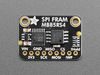
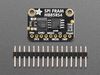
This breakout is built around the Fujitsu MB85RS4MT, a high-performance 4-Mbit (512 KB) SPI FRAM designed for applications that demand fast, byte-addressable, non-volatile memory with extreme endurance.
The MB85RS4MT behaves like SRAM at the interface level — instantaneous reads and writes with no erase cycles, no page boundaries, and no write delays — while retaining data without power. It supports SPI clock rates up to 40 MHz, making it well-suited for high-speed data logging, buffering, counters, and state storage where Flash or EEPROM introduce latency and wear concerns.
With a guaranteed 10¹³ write cycles per byte and data retention rated up to 95 years at room temperature, this FRAM is ideal for systems with frequent updates or unreliable power. Typical use cases include energy meters, industrial sensors, robotics, and low-power embedded systems where data integrity is critical.
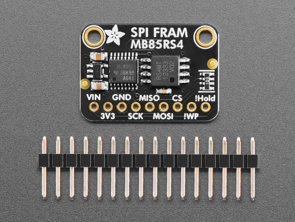
The breakout includes onboard 3.3 V regulation and logic-level shifting, allowing direct use with 3.3 V or 5 V microcontrollers. It is fully assembled, breadboard-friendly, and ships with standard 0.1″ header pins for quick integration.
Specification
| Specification | Details |
|---|---|
| Product Type | SPI Non-Volatile FRAM Breakout Board |
| FRAM IC | Fujitsu MB85RS4MT |
| Memory Capacity | 4 Mbit (512 KBytes) |
| Memory Organization | 524,288 words × 8 bits |
| Interface | SPI (Serial Peripheral Interface) |
| Supported SPI Modes | Mode 0 (CPOL=0, CPHA=0) and Mode 3 (CPOL=1, CPHA=1) |
| Max SPI Clock | 40 MHz |
| Endurance | 1013 writes per byte |
| Data Retention | 10 years @ +85°C, 95 years @ +55°C, 200+ years @ +35°C |
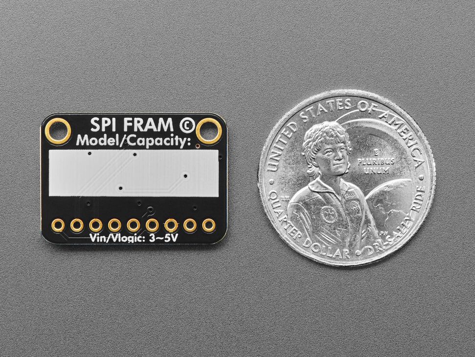
| Operating Voltage (FRAM) | 3.3V logic domain (onboard regulation and level shifting included) |
| Input Voltage | 3V or 5V compatible (VIN pin) |
| Logic Level Compatibility | 3.3V and 5V microcontrollers supported (onboard level shifting) |
| Supply Current | 2.6 mA max @ 40 MHz |
| Operating Temperature | -40°C to +85°C |
| Board Features | 3.3V regulator, logic-level shifting, breadboard-friendly layout |
| Headers | Standard 0.1" header pads (header typically included) |
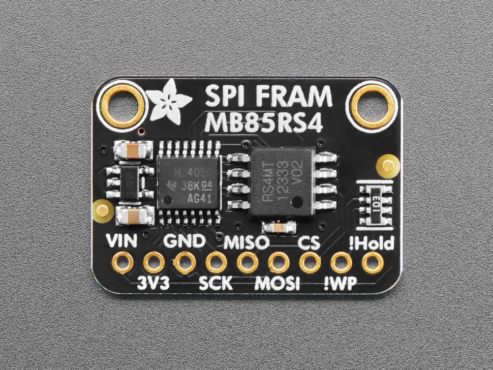
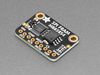
Pinout
| Pin | Function |
|---|---|
| VIN | Power input (3V–5V). Feeds onboard 3.3V regulator. |
| 3V3 | Regulated 3.3V output. Can be used to power external circuits (limited current). |
| GND | Ground reference. |
| SCK | SPI clock input. |
| MOSI | SPI Master Out / Slave In (data input to FRAM). |
| MISO | SPI Master In / Slave Out (data output from FRAM). |
| CS | Chip Select (active low). Enables SPI communication. |
| !WP | Write Protect (active low). Pull low to protect memory from writes. |
| !HOLD | Hold (active low). Pauses SPI communication witho |
Opps
Sorry, it looks like some products are not available in selected quantity.
Reviews
No reviews have been written for this product.